Enabling Fully Automated Testing of SiPh at Wafer Level
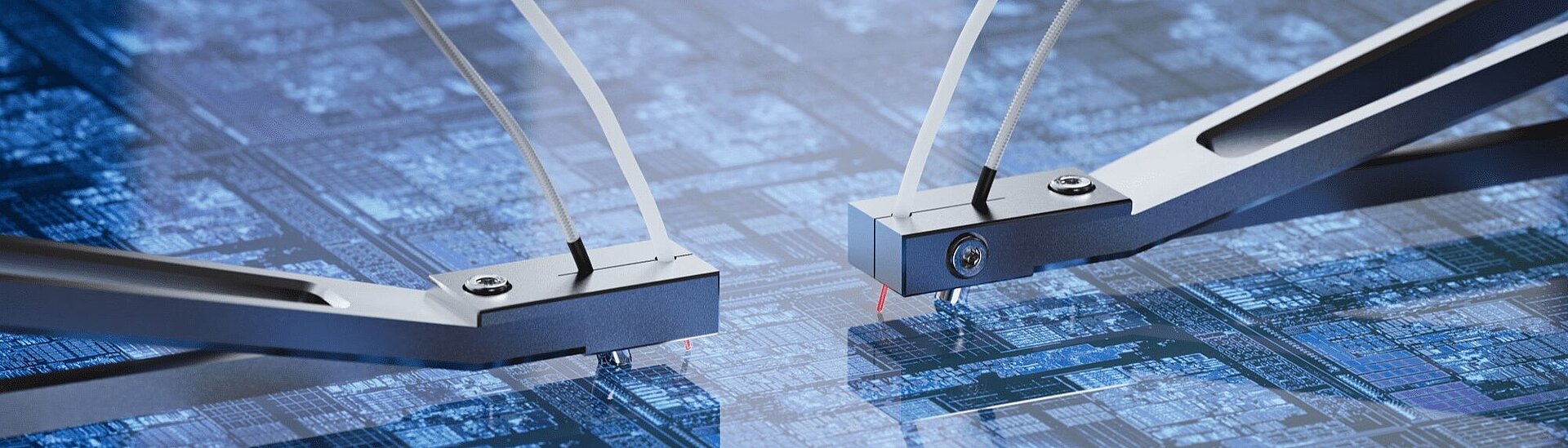
The economical mass production of silicon photonics (SiPh) components requires high-speed alignment with nanometer accuracies: With thousands of photonic structures on one wafer, the faster the alignment of the signal-carrying optical fibers to the photonic circuits, the faster and thus more economical testing becomes. Probing solutions must combine high speed and precision with adequate sensor technologies to avoid direct contact between probe and wafer, thereby preventing particle formation and damage to chip structures.
The integration of photonic elements on a silicon chip or chiplet presents a multitude of challenges for testing technology, starting at wafer level. Photonics alignment systems must be able to react with high flexibility to differing chip designs. Edge emitters, for example, require horizontal alignment of the test fiber, whereas grating couplers require vertical alignment at wafer level. Aligning edge emitters also enables testing at die level. Efficient array alignment helps manage varying alignment requirements and ensures precise, reliable testing across different chip designs. Automation is key to streamlining all these processes, especially at production level.
Engineering Probers: Wafer Testing at the Concept Phase of the Chip Layout
Wafer-level testing supports the development of chip or structure layouts by validating their functionality. During the R&D phase, silicon photonics wafers are tested frequently as designs are revised, new manufacturing techniques are explored, and device performance is optimized. Testing is performed after each manufacturing cycle or after significant design changes to evaluate the impact on device characteristics. Solutions that speed up the alignment process help accelerate product development cycles and reduce time to market significantly.
The engineering phase of SiPh device manufacturing therefore requires high-performance alignment systems to perform subnanometer or nanometer-level precision alignment in six degrees of freedom with low insertion loss, high bandwidth, low crosstalk, and high efficiency. Accurate array alignment plays a crucial role in identifying defects, ensuring high-quality production to optimize manufacturing processes of any figure of merit and to improve yield as well as overall product quality.
Production Probers: SiPh Device Testing in Operation Mode
In wafer-level production probers, silicon photonics devices are tested in high duty cycles and at repeated regular intervals in a 24/7 operating environment. To ensure the consistency and reliability of the silicon photonics devices produced, it is critical to monitor device performance, detect defects, and maintain product quality and yield standards.
Production probers require wafer probing systems with high accuracy and nanometer to micrometer precision to ensure repeatable, reliable testing and characterization across all micro-optical elements, improving yield and overall product quality. High duty cycles and 24/7 operation demand high dynamics and no wear, tear, or maintenance to prevent downtime. Automated wafer probing systems are equipped with advanced software features for data acquisition, analysis, and visualization.
Improving Efficiency, Reliability, and Throughput in SiPh Wafer Testing at Engineering and Production Level
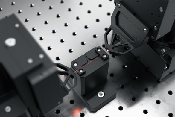
Adapting to changing market requirements and adjusting inspection processes accordingly calls for flexible solutions. FMPA systems from PI position optical fibers and photonic structures in silicon photonic wafer probers within a fraction of a second, reducing testing time for a wafer to hours or days instead of weeks or even months. If your number-one priority in a system is cost rather than speed or performance, we have a solution for that as well: Our modular portfolio enables users to expand their testing capabilities as their needs evolve without significant infrastructure changes. Depending on the application requirements, different alignment solutions from PI are available, detailed next.
Multiple channels, multiple elements, and multiple interacting inputs and outputs, across multiple degrees of freedom, all requiring alignment optimization—a previously time-consuming and expensive task. PI’s Multi-Channel Photonics Alignment (FMPA) systems and unique proprietary alignment algorithms built into the controller automatically enable simultaneous alignments across multiple channels, devices, and degrees of freedom, optimizing overall alignment in one quick step. Time and cost can be reduced by 99 % compared with traditional serial approaches.
When it comes to the alignment of fiber optic devices in high-volume production environments with strict cleanliness requirements, PI offers advanced motion solutions for fast, automated 24/7 operation based on a variety of motor, guiding, and sensor technologies. Complemented by unique proprietary alignment algorithms for parallel optimization of any figure of merit, our solutions can increase throughput by more than one hundred times compared with traditional alignment systems.
Not all processes in photonic device production require maximum throughput and accuracy. Our portfolio also encompasses affordable alignment engines based on modular precision positioning stages that still benefit from PI’s high-performance motion controllers with award-winning embedded alignment algorithms.