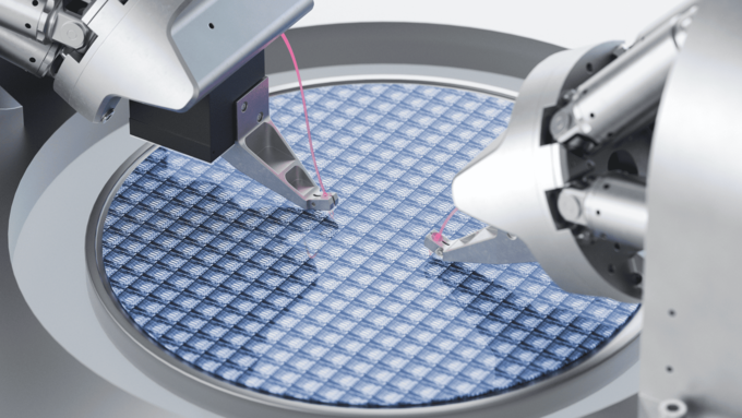
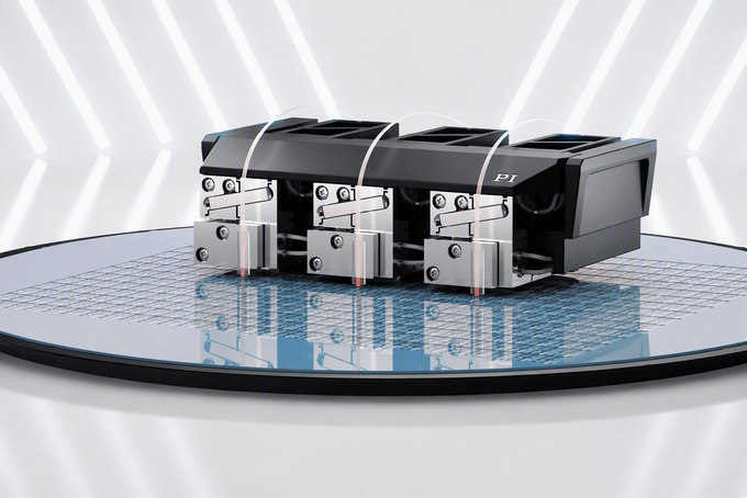
As photonic integrated circuits transition to high-volume manufacturing, testing is becoming critical to scalable and cost-efficient production. In this podcast, Nikta Jalayer, Global Portfolio Director, Photonics, at PI, discusses why optical testing poses fundamentally different challenges from conventional electrical probing and why wafer-level testing is becoming a key enabler for the adoption of photonic technologies in AI and data center applications. In this context, performing these tests at wafer level can help improve yield, throughput, and manufacturing efficiency.
Learn more about
- Why optical wafer-level testing is essential for scaling photonic integrated circuit manufacturing
- How optical testing differs from conventional electrical probing and requires highly precise alignment and stable test environments
- How wafer-level testing helps improve yield, reduce manufacturing costs, and increase throughput in high-volume photonics production
Listen to the full episode!