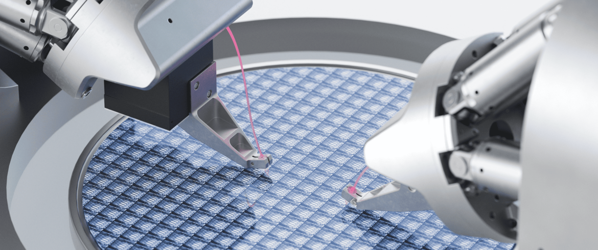
Optical Wafer-Level Probing is essential for testing and manufacturing photonic devices and Photonic Integrated Circuits (PICs). Achieving this requires more than hardware performance—it depends on the seamless integration of motion control, optical feedback, and automation software.
As photonic devices become increasingly complex and production volumes grow, accurate on-wafer characterization is critical for yield and cost efficiency. Optical Wafer-Level Probing enables:
- Measurement of key parameters such as insertion loss, optical power, and wavelength response before dicing and packaging
- Faster device characterization and process optimization during development
- Early defect detection in production to reduce downstream costs and improve yield
At the core of every probing system lies one fundamental requirement: stable, precise optical alignment. Even sub-micron positioning errors can significantly impact coupling efficiency and measurement accuracy.
Achieving this performance requires the interaction of multiple elements: motion systems, controllers, multi-axis synchronization, optical feedback, alignment algorithms, and application software.
PI addresses optical alignment as a fully integrated system challenge. By combining high-precision motion technologies with intelligent alignment software and application expertise, PI helps customers improve measurement accuracy, increase automation, and maximize wafer-test productivity from R&D to high-volume manufacturing.
Key Requirements for Production-Ready Optical Wafer-Level Testing
As PICs transition from R&D to high-volume manufacturing, optical wafer-level test solutions must meet the same manufacturing objectives that have long driven the semiconductor industry: maximizing yield, increasing throughput, reducing cost of test, and enabling scalable production.
The critical requirements include:
- Deliver highly repeatable optical measurements with low uncertainty to ensure reliable device characterization and minimize false positives and false negatives.
- Minimize alignment, positioning, and measurement cycle times while maximizing first-pass measurement success through automated alignment workflows to support high-volume manufacturing.
- Maintain robust optical alignment throughout testing to ensure consistent measurement results across the entire wafer and over extended production runs.
- Seamlessly integrate with automated wafer probers, handlers, MES, and production software to enable lights-out manufacturing and standardized production workflows.
- Maximize equipment uptime through fast recipe changes, automated calibration, minimal operator intervention, and reliable long-term system stability.
Engineering Challenges to Overcome
Achieving these objectives requires solving several complex engineering challenges:
- Maintaining sub-micron positioning precision and repeatability despite vibration, thermal drift, and environmental influences
- Supporting both single-sided and double-sided optical coupling configurations
- Synchronizing multiple motion axes with high accuracy
- Maintaining stable optical coupling throughout the entire measurement cycle
- Meeting semiconductor manufacturing requirements including cleanroom compatibility and low particle generation
- Supporting fast motion profiles and short settling times for high-throughput operation
- Minimizing system footprint while maximizing functionality
Successfully addressing these challenges is essential for achieving accurate measurements, stable processes, and the throughput required for scalable photonic manufacturing.
Application Expertise and Modular System Design
Decades of experience in precision motion control and photonics applications have enabled PI to develop solutions specifically tailored to the requirements of Optical Wafer-Level Probing. PI technologies combine positioning accuracy, long-term stability, repeatability, and dynamic performance with cleanroom compatibility and support for automated test environments.
Recognizing that every application has unique requirements, PI offers varying levels of system integration, from individual motion components to fully integrated alignment subsystems. Depending on the application, solutions can combine precision positioning stages, hexapods, motion controllers, fiber holders, distance sensors, optical power meters, and alignment software into a tailored alignment platform.
This modular approach enables customers to start with individual motion components during research and process development and scale toward highly automated production systems as requirements evolve. Throughout this journey, customers benefit from PI's proven motion-control expertise and application know-how across all stages of photonic device testing.
Accelerating First-Light Acquisition with PI Lightning
One of the most critical contributors to wafer-test productivity is the time required to establish optical coupling. In production environments, every second spent searching for first light reduces equipment utilization and increases test costs. To address this challenge, PI developed PI Lightning, an advanced alignment algorithm specifically designed to accelerate first-light acquisition. By combining intelligent search strategies with PI's high-performance positioning systems, PI Lightning dramatically reduces alignment times compared with traditional scanning approaches. Benefits include:
Instead of spending minutes locating an optical signal, manufacturers can establish stable optical coupling in seconds, significantly improving overall production efficiency.
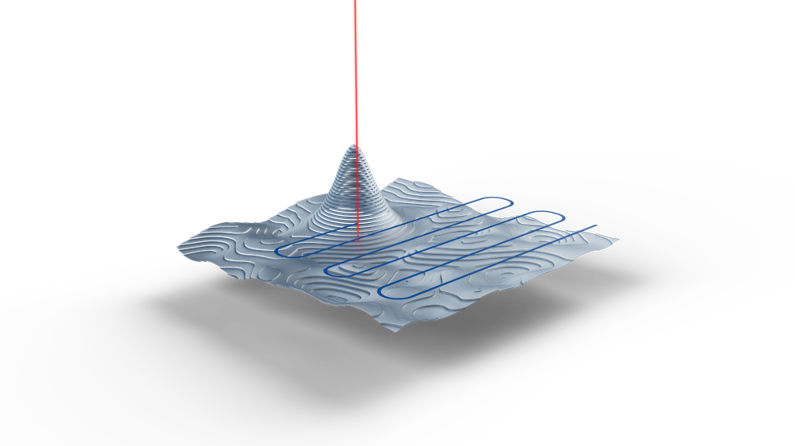
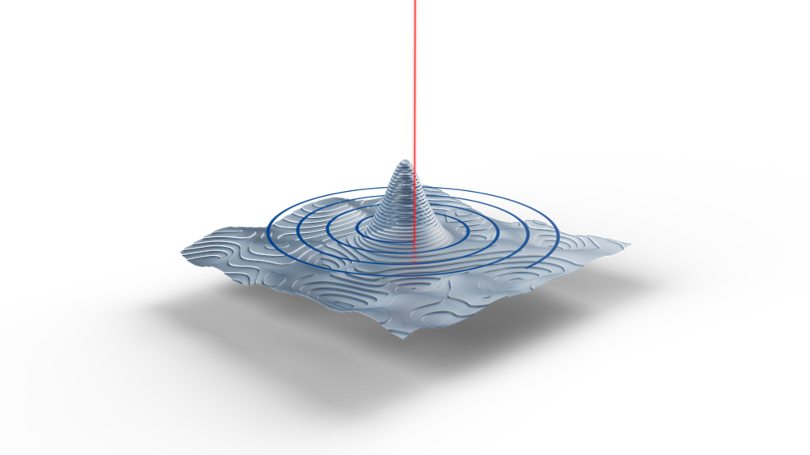
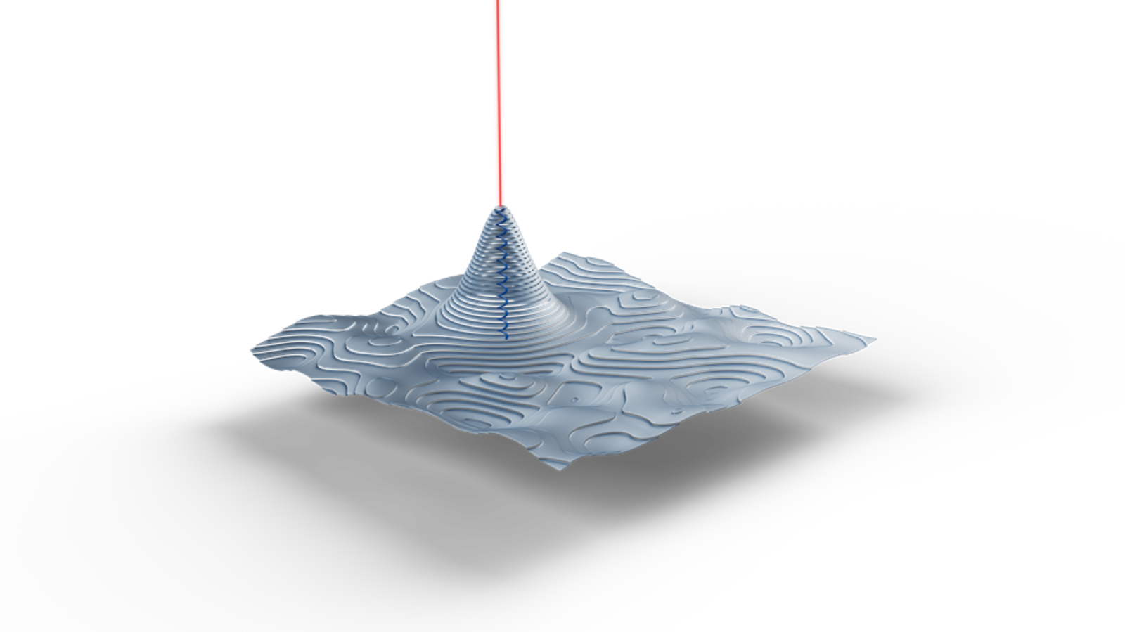
Finding first light using current signal search methods is based on area scans followed by gradient search or layered optimization. Performing spiral scans or sinusoidal raster Scans at a micron-to-submicron scale, however, can require significant time to complete depending on the area that must be searched, whether inputs and outputs need to be simultaneously aligned, and so on.
Scalable Solutions from Lab to Fab
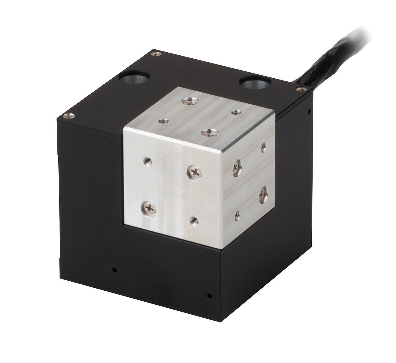
As photonic products move from research to industrial production, alignment requirements change significantly. Researchers require maximum flexibility to evaluate alignment concepts and develop test methodologies. System integrators need solutions that simplify implementation and reduce development effort. Production environments, in contrast, demand high levels of automation, repeatability, and throughput.
To support these diverse requirements, PI offers a scalable portfolio of alignment solutions with varying levels of integration. The >> P-616 family enables flexible development of optical wafer-level probing processes, while the >> F-713 family provides fully integrated single-sided and double-sided alignment solutions for automated wafer testing.

Key Advantages of PI’s Wafer-Level Probing Solutions
Accurate measurements, efficient alignment workflows, and scalable automation are essential for successful Optical Wafer-Level Probing. By combining precision motion technologies, intelligent alignment algorithms such as PI Lightning, and deep application expertise, PI helps customers improve measurement quality, increase productivity, and support the transition from development to production.
Customers benefit from: